VLSI (Very Large Scale Integrated Circuits) is one of the key element to nourish the domestic electronic hardware industry
With the advent of an accelerated pace of changes in the Information Technology (IT) domain, the emergence of the Internet of Things (IoT), Artificial intelligence (AI) gadgetry, Machine Learning (ML), the need for Very Large Scale Integration (VLSI) in chips manufacturing has become inescapable.
VLSI need specific talents and India is desperately in need of teachers as well as skilled manpower. It is unable to fulfil those requirements as most of the talent gets employed abroad or by MNCs in highly paid jobs. In turn, Indian MSMEs and Start-Ups are starved of the VLSI talent, as they are unable to match the pay scales.
MSMEs and Start-Ups are the backbones of industrial manufacturing in India and it is this sector that supports the requirements of the Indian armed forces and employs a large chunk of youth. India certainly needs to take stock of this dichotomy and institute some remedial measures to resolve the problems.
In view of the above, this article will examine the broad contours of VLSI and its importance, skills needed, current situation in India and some suggested measures.
VLSI and It’s Importance
Journey: Transistors, MOSFET, FinFET, VLSI
About 4 decades ago, the world has started witnessing the magic of Transistors. However, due to technical limitations and the size of transistors, a typical number of transistors that could be found in a chip is less than 10,000. For example, a popular Motorola 6800 microprocessor (6.0‐μm feature size), developed in the mid-1970s, contained merely 4100 transistors.
However, with the requirements of larger and faster circuits, VLSI started emerging as a new vector. Today, the number of transistors in very-large-scale integration (VLSI) or the super large‐scale integration (SLSI) chips could reach 10 billion, with a feature size smaller than 15 nm.
There is not much doubt electronics world has experienced a significant advancement for the past 4 decades or so and this could be attributed to rapidly advancing technology enhancing the performance, power, area, cost and ‘time to market’ of an integrated circuit (IC) chips.
When transistors were first introduced in the early 1900s, they were actually made of vacuum tubes. These transistors were relatively large in size and cumbersome to be used. In December 1947, however, three physicists working in the AT&T Bell laboratory attained a remarkable breakthrough in their design, changing the perception one used to have on transistors. Dr John Bardeen, Dr Walter Houser Brattain and Dr William Bradford Shockley, Jr., invented the first point‐contact semiconductor transistor using germanium.
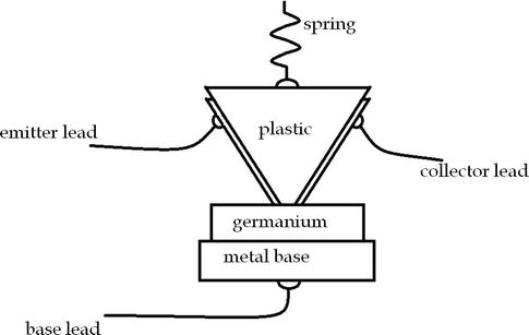
Fig: 1- An early model of the point‐contact transistor. Image Courtesy: intechopen
From these to MOSFET (basically a device that operates like a switch or an amplifier in electronic circuits) to FinFET (with sizes reducing to 22 nm) and now to VLSI (sizes below 15 nm)—it has been an amazing IT journey.
VLSI Design Flow
Generally, the design process of the chip involves three stages namely the (i) behavioural, (ii) logic circuit and (iii) layout representations. At each stage, verification is to be performed at the end before proceeding to the next IC fabrication and IC packaging. Hence, it is common to have repetitions and iterations in the processes. The requisite stages are:-
- Behavioural Representation: At this stage, it is important to specify the functionalities of the device and how it is going to communicate with the exterior. A hardware description language (HDL) such as Verilog HDL or VHDL is used to define the behaviour of the device.
- Logic Circuit Representation: After the HDL codes are successfully simulated, functional blocks from standard cell libraries are used to synthesize the behavioural representation of the design into a logic circuit representation.
- Layout Representation: At the final stage, the physical layout of the design is created. The process starts with floor planning which defines the core and routing areas of the chip. In order to optimize the design, the building blocks are arranged and orientated at their best locations. This process is known as placement. Once this is completed, a routing process is performed to interconnect the building blocks.
- Post Layout Representation IC Fabrication and IC Packaging is done, after which it is ready to be released to the market.
(Sources: Tlelo-Cuautle, 2012 and Yeap and Nisar, 2016)
Importance of VLSI Architecture
The demand and growing sophistication of applications have been continuously pushing the design and manufacturing of integrated circuits and electronic systems to unimaginable levels of complexity. However, this push has also triggered an unprecedented variety of uses. As a consequence of increasing complexity, manufacturers are not only building specific product s but also a wider range of special-purpose systems. This technological ability has become a testament to the growing mastery of both integrated circuit manufacturing and design at one end and increasing demands of customers which test the limits of design and manufacturing at the other. The ability to execute Very Large Scale Integration (VLSI) has allowed the manufacturers to build systems with a very high number of transistors, enhancing the computing power for solving problems (informIT, 2009).
Fig: 2- Complex PCB Design, Image Courtesy: pcb.cadence
It has been observed that this technology is quite ideally suited to the ever-increasing demand for complex electronic devices and systems. In addition to requirements for miniaturization, portability, performance, and reliability, and functionality, VLSI technology will continue to drive electronics advancement. For example, the design/manufacture of the PCB depicted in Fig: 2, with numerous semiconductors, would not be feasible without VLSI technology (Cadence PCB Solutions, ND).
VLSI Technology Advantages and Limitations
As any technology would have, VLSI technology too has its advantages and limitations.
Advantages:
Without VLSI technology, it would be impossible to implement, verify, and test the complex, single-chip electronic systems, that are the foundation of the modern-day information technology revolution. The VLSI Technology offers the following distinct advantages:-
- Reduced size for circuits
- Increased cost-effectiveness for devices
- Improved performance in terms of the operating speed of circuits
- Requires less power than discrete components
- Higher device reliability
- Requires less space and promotes miniaturization
Limitations:
VLSI Technology suffers from some limitations too. They are:-
- Fundamental limitations of design technology.
- More expensive for device designs.
- Lack of training infrastructure
- Limited R and D Resources
(Sources: Bryant et al, 2001, Cadence PCB Solutions, NDa and Kumar, 2017)
Skill Sets Required for VLSI Applications
VLSI field demands high skill set. Some of the important skills which are a pre-requisite for working in VLSI field cover:-
Personal:
- Problem-solving ability
- Ability to think out of the box
- Learning attitude
- Good listening Skills
- The ability of working together
Professional
The VLSI sector is a highly technical field that is totally based on electronics and electrical engineering it demand:
- Branches conducive for working in the VLSI field are EE (Electrical & Electronics) and EC (Electronics & Communication).
- Strong capabilities in circuit analysis, analogue electronics, digital electronics, VLSI CMOS, Verilog, etc.
- Experience in handling projects during engineering related to VLSI or electronics
- Familiarity with EDA tools that are used in chip design.
(Source: Shidling, 2020)
Current Situation in India
- Quality Issues
Experience has shown that the employability of Engineering graduates and their ability to deliver to the VLSI industry expectations, post recruitment has not been up to the mark. It has been observed that it is a problem of both quality and quantity. The quality of VLSI education and the quality of students getting through engineering institutions has been poor. This is because only a few colleges in India have the infrastructure or specific courses related to the VLSI domain. Universities don’t have specific courses related to VLSI in their curriculum.
- Quantity Issues
It has also been observed that the quantity of VLSI engineers available in India is also quite low. Thus the VLSI talent is too expensive to hire. The MSME and the StartUp suffer because of this as they cannot afford the high cost of VSLI talent.
Researchers have determined that some institutes in India provide world-class training to VLSI engineers. However, such talent gets immediately hired by companies abroad or MNCs (Intel/ Qualcomm, Samsung, Western Digital etc.) in India at very high pay packages. Thus many good Institutions like IIT Delhi do not get good faculty or Indian Industry, good VLSI engineers. India is thus in a very peculiar bind that it finds very difficult to produce the VLSI talent it needs (Phadnis and John, 2021).
- Probable Solutions
The solution to the quality issues is to offer good quality VLSI education with live hands-on projects. The solution to the quantity issues is to offer quality VLSI education in more institutes. To address these issues KLE Tech-IESA-SEER has collaborated for promoting skill set requirement through a set of courses. The courses are designed, delivered and assessed by in-house and industry-expert to build competence. The success story is the extensive industrial experience, internship opportunity and job in VLSI core companies.
As per IESA (India Electronics and Semiconductor Association) Indian Government’s Special Manpower Development Program (SMDP) is focused on incentivising the moves from chips to system design and is also providing funds to academic institutions. The Industry also opined that highly skilled industry professionals need to be spared to share their expertise with the students in various academic institutions (Phadnis and John, 2021a).
But such efforts are still inadequate to meet India’s requirements and lot more needs to be done if India wants to remain a global IT powerhouse.
Conclusion and Suggestions
Chips are becoming core to everything around us today and VLSI is the heart of today’s technology revolution. India just cannot afford to lag behind in this field. To become capable and remain relevant in VLSI game India needs to put some measures in place, that too on a fast track mode. Such measures may cover:-
- Creation of more quality institutions that will teach curriculum in Electronics and VLSI.
- Make provision for advanced topics related to VLSI in the curriculum.
- Teach basics of VLSI at 10+2 level.
- Create a pool of VLSI talent which could be shared between the Industry and the academic institutions.
- Incentivise industry to gear up for high end Chip fabrication, thus creating more job opportunities and in turn retaining the talent.
Finally it can be said that India needs to acts fast in this Chips business, before the chips really go down. Jai Hind.
Title Image Courtesy: https://sukhavasisuparshyababu.wordpress.com/
Disclaimer: The views and opinions expressed by the author do not necessarily reflect the views of the Government of India and Defence Research and Studies
References:
- Esteban Tlelo-Cuautle Esteban, Jan 2012, Researchgate, VLSI Design (DOI: 10.5772/2255)
Retrieved from: https://www.researchgate.net/publication/234007956_VLSI_Design, Accessed on 13-14 Apr 2021
2. Kim Ho Yeap Kim Ho, Nisar Humaira, 29 Sep 2016, intechopen, VLSI (DOI: 10.5772/intechopen.69188), Retrieved from: https://www.intechopen.com/books/very-large-scale-integration/introductory-chapter-vlsi,
Accessed on 13-14 Apr 2021
3. informIT, 18 Feb 2018, informIT (Pearson), Digital Systems and VLSI, Retrieved from:
https://www.informit.com/articles/article.aspx?p=1315269, Accessed on 13-14 Apr 2021
4. Cadence PCB Solutions, ND, cadence.com, VLSI Technology: Its History and Uses in Modern Technology, Retrieved From: https://resources.pcb.cadence.com/blog/2020-vlsi-technology-its-history-and-uses-in-modern-technology, Accessed on 13-14 Apr 2021
5. Bryant Randal E, Cheng KTT, Kahng A, Keutzer Kurt, Maly Wojciech P, Newton R, Pileggi L. Rabaey J.M , Sangiovanni-Vincentelli Alberto L, Resaerchgate, Limitations and challenges of computer-aided design technology for CMOS VLSI (DOI:10.1109/5.915378), Retrieved From: https://www.researchgate.net/publication/2985818_Limitations_and_challenges_of_computer-aided_design_technology_for_CMOS_VLSI, Accessed on 13-14 Apr 2021
6. Cadence PCB Solutions, NDa, cadence.com, VLSI Technology: Its History and Uses in Modern Technology, Retrieved From: https://resources.pcb.cadence.com/blog/2020-vlsi-technology-its-history-and-uses-in-modern-technology, Accessed on 13-14 Apr 2021
7. Kumar Seelam Vasavi Sai Viswanada Prabhu Deva, 04 Dec 2017, slideshare, Very Large Scale Integration (VLSI) technology, Retrieved from: https://www.slideshare.net/SeelamVasaviSaiViswa/very-large-scale-integration-vlsi-technology, Accessed on 13-14 Apr 2021
8. Shidling Chetan, 04 Nov 2020, cselectricalandelectronics, Roadmap To Becoming A VLSI Engineer Or Chips Design Engineer, Retrieved From: https://www.cselectricalandelectronics.com/roadmap-to-becoming-a-vlsi-engineer-or-chips-design-engineer/, Accessed on 13-14 Apr 2021
9. Siddamal Saroja V, Shirol Suhas, Hiremath Shraddha, Iyer Nalini. Jan 2020, Reserachgate, Towards Sustainable Integrated Model for Skill Development: A Collaborative Approach (DOI:10.1016/j.procs.2020.05.099), Retrieved From: https://www.researchgate.net/publication/342226259_Towards_Sustainable_Integrated_Model_for_Skill_Development_A_Collaborative_Approach, Accessed on 13-14 Apr 2021
10. Phadnis Shilpa and John Sujit, 14 Apr 2021, Times of India Print Edition, Why India needs a lot more talent that can craft Chips, Accessed through Print edition on 14 Apr 2021.